

Description
Introduction
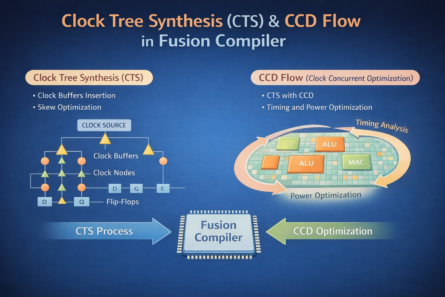
Fusion Compiler is an advanced electronic design automation (EDA) tool used for digital implementation, including synthesis, placement, routing, and optimization. Clock Tree Synthesis (CTS) and Clock Concurrent Optimization (CCO) or CCD flow in Fusion Compiler ensure balanced clock distribution and optimized timing closure in high-performance chip designs. This training focuses on CTS fundamentals, clock optimization strategies, and CCD flow integration for efficient and reliable IC design.
Learner Prerequisites
- Basic understanding of digital electronics and VLSI design
- Familiarity with CMOS technology concepts
- Knowledge of static timing analysis (STA) basics
- Awareness of clock distribution and timing concepts
- Basic understanding of EDA tools and chip design flow
- Interest in semiconductor design and physical implementation
Table of Contents
1. Introduction to Clock Tree Synthesis and CCD Flow
1.1 Overview of CTS in digital design
1.2 Importance of clock distribution networks
1.3 Introduction to CCD (Clock Concurrent Design) flow
1.4 Role of Fusion Compiler in CTS and CCD
1.5 Real-world applications of clock optimization
2. Clock Tree Fundamentals
2.1 Basics of clock networks
2.2 Clock skew and latency concepts
2.3 Clock sources and sinks
2.4 Clock buffering techniques
2.5 Impact of clock design on performance
3. Clock Tree Synthesis Flow in Fusion Compiler
3.1 Overview of CTS flow stages
3.2 Clock definition and specification setup
3.3 Clock tree construction process
3.4 Clock balancing techniques
3.5 CTS constraints and objectives
4. Clock Concurrent Design (CCD) Flow Overview
4.1 Introduction to CCD methodology
4.2 Integration of CTS with placement and routing
4.3 Benefits of concurrent optimization
4.4 CCD flow stages in Fusion Compiler
4.5 Comparison of CTS and CCD approaches
5. Clock Tree Optimization Techniques
5.1 Reducing clock skew
5.2 Minimizing clock latency
5.3 Buffer insertion strategies
5.4 Clock gating techniques
5.5 Power optimization in clock networks
6. Timing Analysis in CTS and CCD
6.1 Static timing analysis integration
6.2 Setup and hold timing checks
6.3 Clock uncertainty considerations
6.4 Slack analysis in clock paths
6.5 Timing closure strategies
7. Placement and Routing Interaction with CTS
7.1 Impact of placement on clock trees
7.2 Routing constraints for clock networks
7.3 Congestion handling techniques
7.4 Clock-aware placement strategies
7.5 Post-routing clock optimization
8. Debugging Clock Tree Issues
8.1 Identifying clock skew problems
8.2 Fixing timing violations
8.3 Analyzing CTS reports
8.4 Common clock design issues
8.5 Iterative debugging flow
9. Power and Performance Optimization
9.1 Power-aware CTS design
9.2 Reducing dynamic power in clock trees
9.3 Trade-offs between power and performance
9.4 Clock gating optimization
9.5 Energy-efficient design techniques
10. Real-World Applications of CTS and CCD
10.1 Microprocessor clock design
10.2 High-performance computing chips
10.3 AI and GPU architectures
10.4 Mobile SoC clock optimization
10.5 Automotive electronics systems
11. Advanced CTS and CCD Techniques
11.1 Machine learning in clock optimization
11.2 Advanced buffering strategies
11.3 Multi-clock domain management
11.4 Hierarchical clock tree design
11.5 Future trends in clock synthesis
Conclusion
This training provides a complete understanding of Clock Tree Synthesis and CCD flow in Fusion Compiler. It explains how clock networks are designed, optimized, and analyzed for high-performance chips. Moreover, learners gain practical knowledge of timing, placement, and power optimization techniques. As a result, they are prepared to handle advanced clock design challenges in modern semiconductor systems.


Reviews
There are no reviews yet.